P5777 [CTSC2001] Optimal Design of Logic Circuits
Description
Professor W teaches a “Digital Logic” course in the Department of Computer Science at University T, mainly about how to design logic circuits. One day, Professor W assigned a lab: design and implement a logic decoder circuit with $4$ inputs and $4$ outputs. Designing such a circuit is not difficult by itself, but the professor imposed the following requirements:
1. You may only use gate components with $2$ inputs and $1$ output, and the available types and quantities of gates are given.
2. Use as few gate components as possible.
These requirements stumped the whole department, so student Q came to you, who are participating in CTSC (China Team Selection Contest), and hopes you can write a program to automatically find a wiring scheme that satisfies the requirements.
In digital logic, all signals can be considered to have only two values: “high level” and “low level”, represented by $1$ and $0$, respectively.
The behavior of a gate component is uniquely determined by its input/output truth table. A truth table describes the relationship between input signal levels and the output signal level. For example, the symbol and truth table of an “AND gate” are shown below:
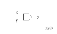
|X|Y|S|
|:-:|:-:|:-:|
|0|0|0|
|1|0|0|
|0|1|0|
|1|1|1|
In the figure above, if both inputs $X$ and $Y$ of the AND gate are at high level $1$, then the output $S$ is also high level $1$; otherwise, the output $S$ is low level $0$.
Assume that all gate components provided in this lab have symmetric inputs, meaning that swapping the two inputs does not change the output. However, if an input pin of a gate is left floating (i.e., no input signal is connected), then the output is meaningless.
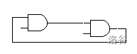
When wiring the circuit, the output pin of a gate may send its signal to the input pins of multiple other components, but each input pin of a gate may receive a signal from only one output pin, as shown below:
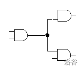

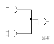
Among them, the first two wiring methods are allowed, while the last one is not allowed.
In addition, signals must be transmitted in only one direction. That is, the output of a gate cannot return (directly or indirectly through other gates) to an input of the same gate. The following figures show two forbidden wiring methods:
The decoder circuit you are required to design is a logic circuit with four inputs and four outputs. The input-output relationship of this decoder is given by a truth table, i.e., for each input combination, the states of the four output pins are specified. Clearly, there are $2^4=16$ possible input combinations. For example, a simple $2$-input, $2$-output decoder circuit built from the AND gate above is shown below (where A1, A2 are inputs, and Y1, Y2 are outputs):
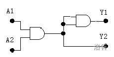
|A1|A2|Y1|Y2|
|:-:|:-:|:-:|:-:|
|0|0|0|0|
|1|0|0|0|
|0|1|0|0|
|1|1|1|1|
Input Format
The first line contains a positive integer $n(n\le 5)$, the number of component types. The next $n$ consecutive lines each describe one type of component. For an integer $1\le k\le n$:
Line $k+1$ contains four integers separated by spaces: $m_k,Y_{00},Y_{01},Y_{11}$.
Here, the positive integer $m_k$ is the number of available components of type $k$ (where $k$ is the type index). The total number of all components will not exceed $10$ (the lab budget is limited). $Y_{ij}$ denotes the output when the two inputs are $i$ and $j$, respectively. That is, $Y_{00},Y_{01},Y_{11}$ are three values each being either $0$ or $1$, representing the output when both inputs are $0$; when one input is $0$ and the other is $1$; and when both inputs are $1$.
Lines $n+2$ to $n+17$ give the truth table of the integrated circuit to be constructed. Each line contains $8$ numbers, each either $0$ or $1$. The first four numbers correspond to the signals on the four input pins (numbered $1\sim 4$) in order; no two lines have exactly the same first four numbers. The last four numbers correspond to the signals that the four output pins should produce (in order) when the inputs are the given first four numbers.
Output Format
The first line contains one word, `Yes` or `No`. If there exists a design that satisfies the requirements, output `Yes`; otherwise output `No`.
If the first line is `No`, the output ends.
Otherwise, the second line contains one non-negative integer $p$, the minimum number of gate components needed. The next $p$ lines each describe the wiring of one gate in the circuit. Each line contains four positive integers separated by spaces: $S ,K, A, B$. Here, $S$ is the index of this gate (all used gates are numbered $5\sim p+4$, while $1\sim 4$ are reserved for the four input pins). $K$ is the component type index (numbered $1\sim n$ in the order of the input). $A$ and $B$ are the indices of the gate or decoder input pin connected to the two input pins of this component, respectively (where $A
Explanation/Hint
#### Sample Explanation
The wiring scheme corresponding to the sample is shown below:

Translated by ChatGPT 5